A tiny dark spot on a display is not always a dead pixel. It can be a stuck sub-pixel, trapped dust, surface dirt, a pressure mark, or a small panel defect. The right test is simple: change the background color, change your viewing angle, and check whether the spot stays locked to the pixel grid.
Start with the Dead Pixel Test and the White Screen Test. A clean solid background makes small defects easier to classify.
Clean the Surface First
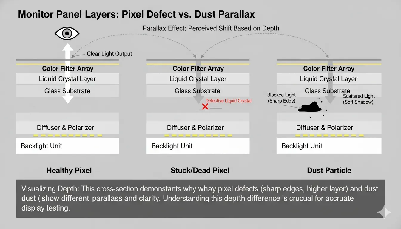
Before diagnosing the panel, rule out surface dust. Turn the screen off, use a clean microfiber cloth, and avoid hard pressure. If the spot disappears, it was on the surface. If it remains in the same place, continue testing.
Do not scrape the screen. Matte coatings and glossy laptop panels can scratch more easily than they look.
Use Color Screens to Classify the Spot
Different backgrounds reveal different defects. A black dot on white may be a dead pixel or dust. A red, green, or blue dot on black is more likely a stuck sub-pixel. A blurry or irregular mark may be dust, coating damage, or pressure-related mura.
| Test screen | Useful for finding | What to notice |
|---|---|---|
| White | Dark pixels, dust, dirt | Sharp grid-like dot vs soft-edged speck |
| Black | Bright stuck pixels, glow, bleed | Colored or white points |
| Red / Green / Blue | Sub-pixel failures | Defects visible on only one channel |
| Grey | Pressure marks and uneven patches | Clouding or soft stains |
Try the Viewing-Angle Check
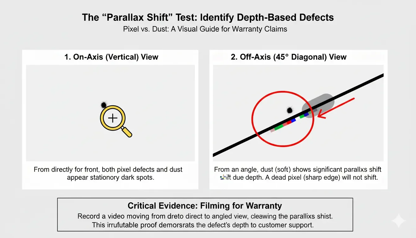
A real pixel defect stays aligned with the pixel grid. Trapped dust or a mark in another layer may appear to shift slightly when you move your head. Sit close enough to see the spot, then move left and right while keeping the test pattern still.
This is not perfect on every display, but it is a useful clue. If the spot has soft edges and changes relative to nearby pixels, avoid calling it a dead pixel too quickly.
Use Photos Carefully
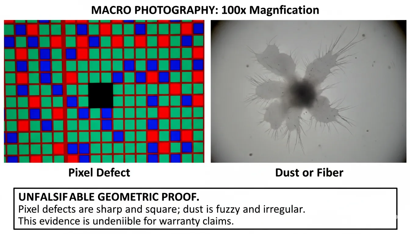
A macro photo can help, but focus matters. Tap to focus on the pixel grid, not on the reflection or the glass surface. Take one straight-on photo and one slight-angle photo. If you contact support, describe what you can verify rather than overstating the cause.
Conclusion
The easiest way to separate a dead pixel from dust is to combine solid colors with angle and focus checks. A sharp defect locked to the grid is more likely a pixel issue. A soft spot that shifts or changes with angle may be dust, dirt, or another layer defect.
FAQ
Can dust be trapped inside a monitor?
Yes, but it is less common than surface dirt. If a speck remains after cleaning and appears below the surface, it may be internal debris or another panel-layer issue.
What color is best for finding dead pixels?
White is best for dark dead pixels, black is best for bright stuck pixels, and red/green/blue screens help isolate sub-pixel problems.
Should I try to fix dust with pixel repair software?
No. Pixel repair software only changes pixel colors; it cannot move dust or repair pressure marks.
Related Tests and Guides
Start with a White Screen
A clean white background makes dark dots and dust easier to inspect.
Open White Screen Test